 HLayout
Process setup
Your layer stack in print order, film thicknesses, design rules, resistor inks and DRC rule sets, saved as a technology file your team reuses on every job.
 Thick-film hybrid circuit layout CAD
HLayout designs the printed conductors, dielectric, resistor inks and glaze of a thick-film hybrid on its ceramic substrate, with packaged parts or wire-bonded bare dies. It takes a KiCad netlist in and sends Gerbers, bond diagrams, assembly drawings and 3D models out.
Free and open source · GPL-3.0 · Windows, Linux and macOS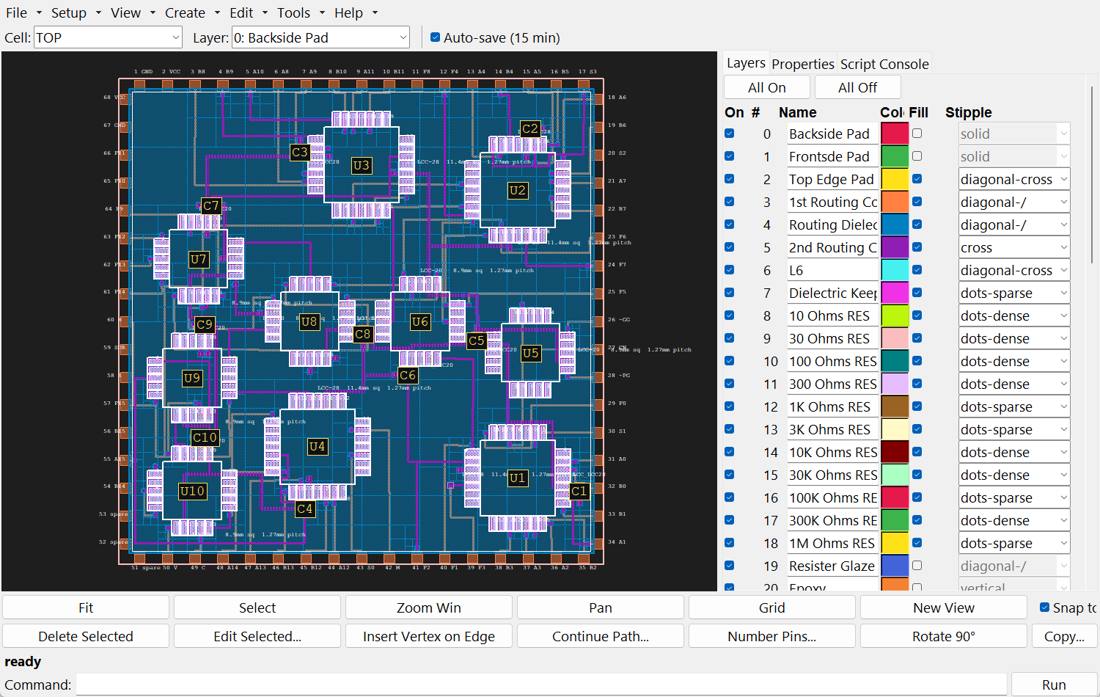
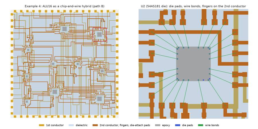
Up to 64 GDSII layers, each given a role: conductor, dielectric, resistor ink, glaze, epoxy, die pads, wire bonds. Top views, 3D models and thermal analysis all stack them as they are fired.
The Resistor Designer sizes each resistor from value, tolerance, power and ink, and the trim simulator models plunge and L-cut laser trimming.
After routing, the dielectric sheet is rebuilt inside the I/O ring with a window at every via.
Seven stages from circuit diagram to the files a print line, die bonder and test station need. The open-source tools are called from inside HLayout and their results come straight back into the design.
Ref-des, pin and die-pad numbers, power nets.
KiCadLayers, libraries, bare dies, printed resistors.
HLayoutAuto Place from the netlist on a 50 µm grid.
HLayoutNet names and a wire bond from every die pad.
HLayoutTwo conductors with vias, or one with jumpers.
FreeroutingDRC, netlist extraction, thermal, trim.
HLayoutGerber, DXF, pick and place, drawings, 3D.
FreeCADKiCad .net · GDSII · Specctra DSN/SES · Gerber RS-274X · DXF · STEP · CSV · KiCad .pos
Your DRC rules set the widths and clearance. Wire-bond landings become bond fingers. The ALU16 chip-and-wire build routes 85 of 85 nets.
Single-conductor hybrids routed with wire-bond jumpers, plus a bond diagram CSV in bonding order for the wire bonder.
Shortest weighted net length with power and ground counted, hot parts kept apart, and straight-line interconnects that follow every drag.
Widths, spacings, substrate-edge clearance and wire-bond length and angle, then copper connectivity compared against your nets.
Steady-state conduction through substrate and films gives each resistor, die and part a temperature against its limit, and a trim simulator shows plunge and L-cut trims step by step. See both tools
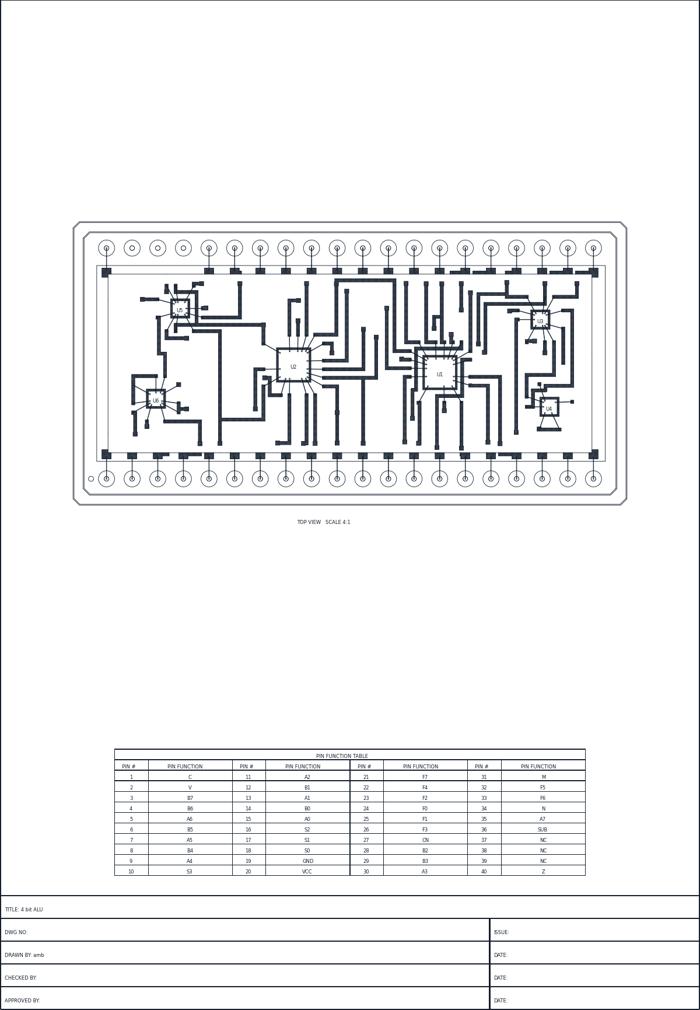
Gerber per print layer, DXF, pick-and-place centroids, test netlists and a one-step assembly drawing with pin, resistor and bond tables.
An 8-bit ALU built from six bare dies (two 54AS181 ALU slices and four 54LS gates) wire-bonded onto a two-conductor thick-film substrate, sealed in a 40-pin Kovar DIP package. 46 nets, placed by Auto Place from the netlist and routed with Freerouting.
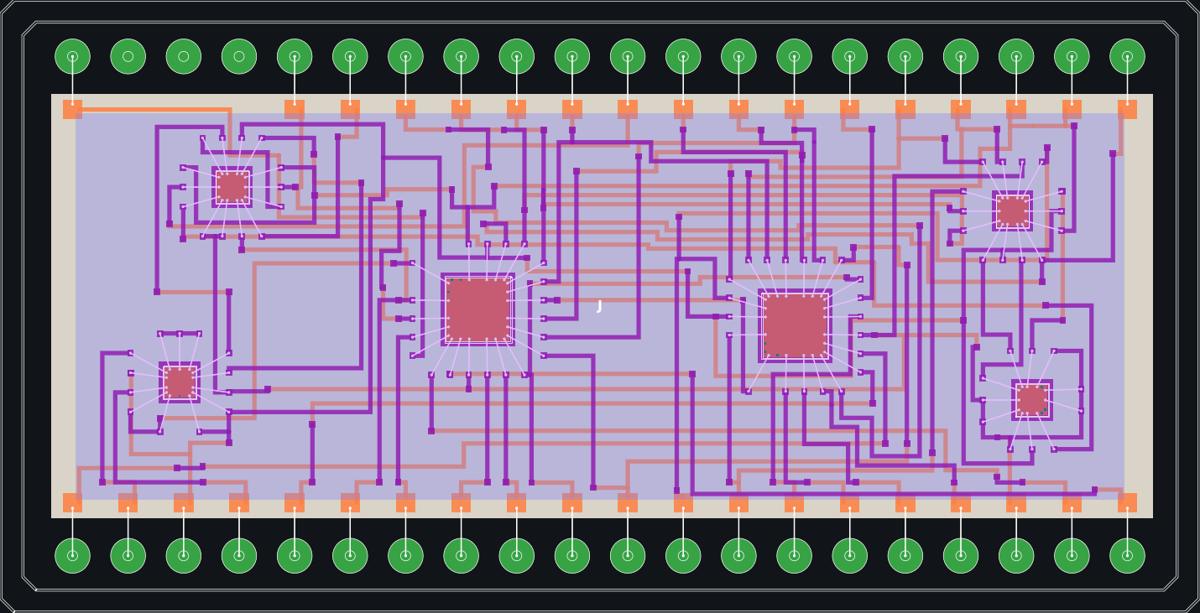
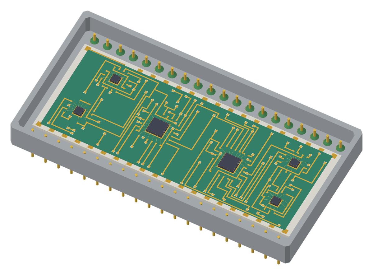
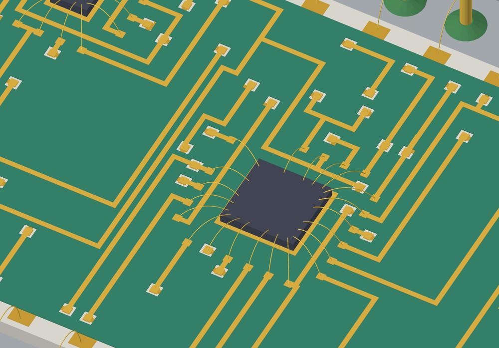
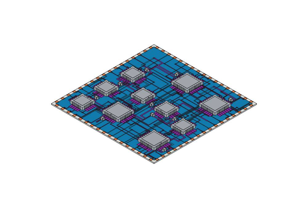
Export the design to FreeCAD as one solid per film at its fired thickness, with real STEP bodies for chip capacitors, SOT and LCC packages, Kovar headers and bare dies. The SolidCraft view writes STEP, 3MF, STL or OBJ.
HLayout is free to use. When you need it adapted to your line, extended with your own tools, or a design laid out for you, the author offers paid help built on the same open-source code.
Tell us about your process, the parts you use and what you want HLayout to do.
Your layer stack in print order, film thicknesses, design rules, resistor inks and DRC rule sets, saved as a technology file your team reuses on every job.
Footprints, bare-die cells with numbered pads, headers and packages, each with a matching STEP model for the 3D view.
New tools, import and export formats, router rules or scripts for your workflow. Work built into HLayout stays open source under GPL-3.0.
From your KiCad schematic to placement, routing, DRC, thermal check, Gerbers, bond diagram and assembly drawing.
Hands-on sessions for your designers using your own parts and rules, and priority help when something stops your line.
HLayout is free, open-source layout CAD for thick-film hybrid circuits and chip-and-wire microelectronic modules. It draws the printed conductors, dielectric, resistor inks and glaze on a ceramic substrate, places packaged parts and bare dies, routes them, checks the design and writes the manufacturing files.
A thick-film hybrid is a circuit whose conductors, insulating dielectric and resistors are screen-printed as pastes on a ceramic substrate, usually alumina, and fired. Chip components, packaged parts and bare semiconductor dies are then attached; bare dies are connected with wire bonds, which is called chip-and-wire assembly.
Yes. Draw the schematic in KiCad and export the netlist; HLayout reads it, places the parts with Auto Place and routes with Freerouting through a Specctra DSN/SES round trip. Die pads and pins can be numbered or named, such as E, B and C for a transistor die.
Yes. The Resistor Designer sizes each resistor from its value, tolerance and power: it picks the body width for the power, an aim value below target for laser trimming, the ink and the number of squares, then places the ink, terminations, glaze and dielectric keep-out. A trim simulator shows plunge and L-cut trims.
Gerber RS-274X for every print layer, DXF, pick-and-place files, bond lists for the wire bonder, test netlists, an assembly drawing with title block and pin table, and a 3D model of the fired substrate and parts for FreeCAD with STEP models.
Yes. Design rule checks cover track widths, spacing, substrate-edge clearance and wire-bond length and departure angle. Netlist extraction compares the drawn copper and bonds with the schematic, and a thermal analysis estimates die and resistor temperatures.
HLayout is free software under the GNU GPL v3.0 or later, with the full source on GitHub. Installers are available for Windows, Linux (Debian/Ubuntu) and macOS, and it can also run from source with Python.
Yes. A three-day hands-on training course takes an 8-bit ALU chip-and-wire design from netlist to Gerbers and 3D, and process setup, part libraries, custom features, layout design and support are available from support@h-layout.co.uk.
Free and open source under GPL-3.0. Installers for Windows, Linux and macOS, built from the public source by the project's CI.
DownloadPick your operating system. Each installer bundles Python and every library HLayout needs, so there is nothing else to install before you start drawing.
Current release All releases and notesWindows 10 or 11, 64-bit.
Debian, Ubuntu and derivatives, x86-64.
macOS on Apple silicon (M1 or later).
HLayout is a Python application. With Python 3.10 or later and Tkinter you can run it on any system, including Intel Macs and non-Debian Linux.
# Debian/Ubuntu only: sudo apt install python3-tk
git clone https://github.com/alvinmb/Hlayout.git
cd Hlayout
pip install -r requirements.txt
python hlayout_app.py hlayout/examples/notch_filter.gds
HLayout runs on its own. These free tools add schematic capture, autorouting and 3D; install the ones you need.
| Tool | Used for | Notes |
|---|---|---|
| KiCad | Schematic capture and the netlist that Auto Place reads | open source Export with File → Export → Netlist. |
| Freerouting | Autorouting two-conductor and chip-and-wire designs | open source Use the Java build; a .jar needs Java 25 or later. |
| FreeCAD | 3D model of the fired stack; building the STEP part library | open source Run the exported .FCMacro, or freecadcmd headless. |
| Claude | Driving HLayout through its built-in MCP server | optional Tools → MCP Server (Claude) starts the bridge. |
HLayout is free software under the GNU General Public License v3.0 or later: you can use, study, change and share it, and the full source is on GitHub. The chip-and-wire router is a fork of Freerouting, also GPL-3.0.
Free code signing provided by SignPath.io, certificate by SignPath Foundation. Signing starts with the first release after the project is accepted; earlier installers are unsigned.
Committers and reviewers: Alvin Brown. Approvers: Alvin Brown. Only release builds made by the project's GitHub Actions workflow from its public source are signed, and each request is approved by hand.
This program will not transfer any information to other networked systems unless specifically requested by the user or the person installing or operating it.
Help → Report Bug saves its report on your computer and opens a GitHub issue only when you ask. The MCP bridge is off until you turn it on and listens only on this computer. Freerouting, installed separately, is run with its analytics turned off.
This website uses Google Analytics only if you accept analytics cookies. It counts page visits and downloads to show which pages are useful; it does not identify you and is not used for advertising. Without your consent no analytics cookies are set and nothing is sent to Google.
Windows: Settings → Apps, or Uninstall HLayout in the Start menu. Debian/Ubuntu: sudo apt remove hlayout. macOS: drag HLayout from Applications to the Bin.